 Simulation of 3D semiconductors has the potential to be extremely useful when developing and improving semiconductor technology by reducing the amount of experimentation and fabrication required to design complex devices. Modeling 3D devices is challenging as the length scales that must be resolved, combined with the nonlinear nature of semiconductor physics phenomena, often require computationally expensive simulations. Here, we share an example simulation of a 3D bipolar transistor and important advice for effective modeling of 3D semiconductors with COMSOL Multiphysics.
Bipolar Transistors
Originally invented in the late 1940s, bipolar transistors were widely used in the first integrated circuits. Although modern field-effect devices have largely replaced bipolar transistors in digital logic circuits, bipolar transistors remain widely used for analog applications. They are particularly widespread in power regulation circuitry, where they are used as switches and current amplifiers.
Simulation Considerations
In order to ensure that a simulation effectively captures all the required physics to give an accurate result, it is important to understand the processes that need to be included in the model. These could vary depending on the configuration of the device and the situation in which it is intended to operate. It is always a good idea to ensure that a model gives satisfactory reliability and accuracy while minimizing the complexity of the problem.
This is particularly important for 3D semiconductor simulations, where models created using non-recommended techniques can take many days to solve or possibly never converge.
In this blog post, I will walk you through the process for setting up a 3D semiconductor model of a bipolar transistor device. First, I will introduce and explain the operation of the device and the important physical processes that must be included. I will also discuss the measures needed to effectively include them within the model.
Doping Structure and Device Symmetry
 Like many semiconductor devices, doping is critical to the operation of bipolar transistors. There are two kinds of doping: p-type doping, where a region has extra holes, and n-type doping, where a region has extra electrons.
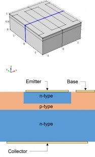
A bipolar transistor consists of three regions of alternating p-type and n-type doping. Although there are two possible doping structures, n-p-n or p-n-p, we will focus on the n-p-n configuration as this is the most common variety. The n-p-n structure is formed by sandwiching a p-type layer between two n-type layers. The device can be considered to have three different regions known as the emitter, base, and collector. Each region can be individually electrically addressed via three separate metal contacts, which are labeled according to the region that they are connected to.
A schematic of the n-p-n doping structure, device regions, and electrical connections is shown here:
Geometry and structure of the bipolar transistor device. Top: The geometry of a bipolar transistor device represented in the COMSOL Multiphysics simulation software. Bottom: Cross section through the device taken along the z-x plane, highlighted by blue edges in the upper image. The n-p-n doping pattern is labeled, along with the electric contacts that connect to the emitter, base, and collector regions.
Due to the alternating doping of the three regions, the bipolar transistor forms two back-to-back p-n junctions that share the base region. The behavior of carriers as they encounter these p-n junctions is crucial for the operation of the bipolar transistor.
Throughout the rest of this example modeling process, I will present suitable steps for including all the relevant physics needed to describe this behavior in a computationally efficient way.
") Planes of Symmetry
Planes of Symmetry
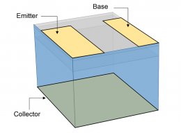
The first question to ask yourself when designing a 3D semiconductor model is: “Can I use symmetry to reduce the model size?”
Many kinds of devices have planes of symmetry, rotational symmetry, or even axisymmetric geometry. If at all possible, using axisymmetric designs is recommended, as this can reduce a 3D simulation down to 2D. An example of the axisymmetric modeling of a cylindrical field-effect transistor can be found here.
The device we want to model in this example has two planes of symmetry that bisect the device in the x-z and y-z planes. This means that we only need to model one quadrant. In the figure below, the upper-right quadrant has been selected:
Geometry required by the model. Due to the planes of symmetry, which are highlighted in blue, only one quadrant of the entire device needs to be included. This reduces the size of the model, allowing it to be solved in a shorter amount of time and with less memory. The metal contacts are applied to surface boundaries as indicated.
Ensuring that Doping Profiles Are Resolved
 After creating the smallest model geometry that symmetry allows, the next question for consideration is: “What resolution do I need to reliably capture the physics within the model?”
Obviously, the geometry dimensions of the device need to be sufficiently resolved. However, the required physical processes often take place on a length scale that is much smaller than the geometry features. For semiconductor models, ensuring adequate resolution can be a challenge, as the various physical processes that are involved often require very different length scales. To make things more complicated, the spatial resolution required to adequately describe many processes can vary drastically throughout the device and can even vary as a function of other model parameters, such as the applied voltages.
A good place to start is to ensure that the doping profiles are resolved. This is because in regions where the dopant concentration changes rapidly, other quantities often undergo drastic variation as well. Thankfully, ensuring that the doping profiles are resolved is relatively straightforward, as the dopant distribution is user-controlled and does not vary when other model parameters change.
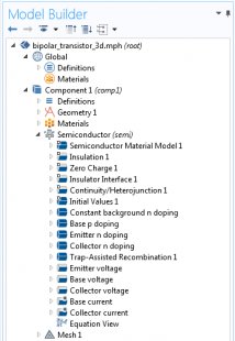
The COMSOL Multiphysics simulation environment provides convenient tools for easily viewing the doping throughout devices. It is a good practice to use the Get Initial Value option available from the Study node, since the dopant concentration is an analytic function that can be computed and visualized without solving the semiconductor equations. The initial value of the doping can then be plotted to help set up a suitable mesh for the full computation.
Below, I have added a 3D volume plot of the doping throughout the model, along with a line cut of the dopant concentration taken along a vertical cut through the center of the device.
Dopant distribution throughout the bipolar transistor device. Left: 3D visualization of the doping throughout the model geometry. The red area in the front-top corner is the n-type emitter region. Due to the order of magnitude variation in the dopant concentration, which is typical of semiconductor devices, it is difficult to see the three different doping regions. Right: Line cut of the dopant concentration taken along the red line in the left-hand image. The logarithmic scale allows the n-p-n doping pattern to be clearly seen and each region is labeled. Note that the dopant concentration varies within each region but the most rapid changes in dopant concentration occur around the emitter-base and collector-base p-n junctions.
Share this Post
latest post
-
 Energy released in nuclear fusion October 31, 2017
 -
 Nuclear fusion as an energy source October 29, 2017
 -
 Nuclear fusion clean energy October 27, 2017
 -
 Order of magnitude estimate project Management October 25, 2017
 -
 Science Workshops October 23, 2017
 -
 States of matter Plasma examples October 21, 2017
 -
 What gas is the Sun made of? October 19, 2017
 -
 U.K. Scientists October 17, 2017
 -
 Three orders of magnitude October 15, 2017